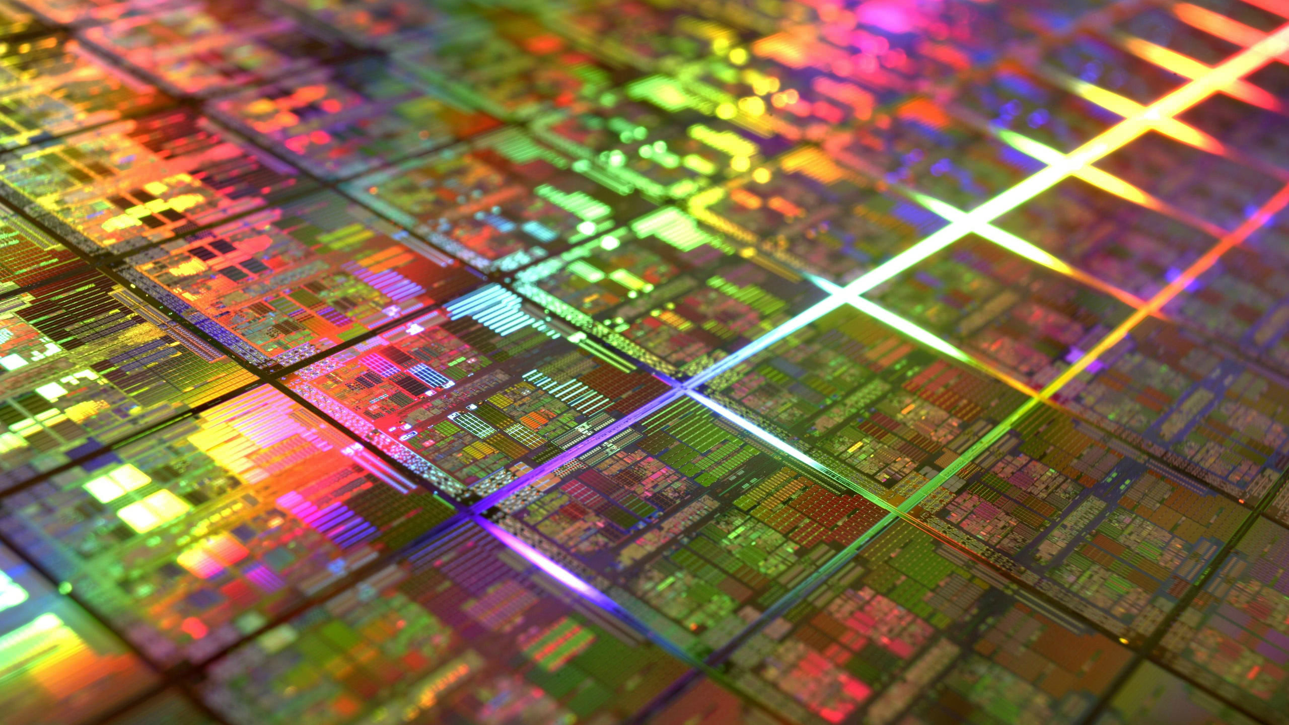
The silicon wafer, a fundamental component in the realm of electronics, serves as the substrate for countless integrated circuits that power the modern technological landscape. A thin, disc-shaped slice cut from a larger ingot of pure crystalline silicon, these wafers undergo a meticulous manufacturing process to ensure the highest standards of purity and perfection. The silicon’s crystalline structure, crucial for optimal electronic performance, is a result of controlled cooling and solidification during the wafer’s formation. The size and thickness of these wafers vary based on the intended application, ranging from a few inches to larger diameters, with nanometer-scale thicknesses to accommodate the intricate circuitry.
The significance of the silicon wafer lies in its role as the canvas upon which the intricate dance of transistors, capacitors, and resistors takes place. Through a series of photolithography and etching steps, microscopic patterns are imprinted onto the wafer’s surface, defining the pathways for electrical currents. Dopants, introduced during the manufacturing process, modify the silicon’s conductivity, transforming it into the essential building blocks of semiconductors. The silicon wafer becomes a symphony of precision, with each layer and pattern contributing to the functionality of the final electronic device. As technology advances, the demand for smaller and more powerful electronic components continues to push the boundaries of what silicon wafers can achieve, making them the silent heroes of our interconnected and technologically-driven world.